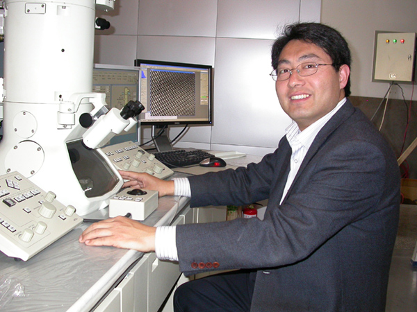
Prof. Yiqian WANG
Vice Dean,College of Physics,
Deputy Director, Cultivation Base for State Key Laboratory,
Qingdao University,
No. 308 Ningxia Road,
266071, Qingdao, P. R. China
Tel.: +86-532-83780318
E-mail:yqwang@qdu.edu.cn
EDUCATION
Sept., 1998-July, 2001 Institute of Physics,
(Ph.D) Chinese Academy of Sciences, China
Sept., 1995-March, 1998 Department of Material Science & Engineering,
(Master) Zhejiang University, Zhejiang Province, China
Sept., 1991-July, 1995 Department of Applied Chemistry,
(Bachelor) Qingdao University, Shandong Province, China
WORK EXPERIENCE
August 2013---present Vice Dean, College of Physics, Qingdao University, China
June 2008---present Professor, Ph.D. adviser, Cultivation Base for State Key Laboratory, Qingdao University, China
October 2006-May 2008 Research Associate, Dept. of Materials, Imperial College London, UK
October 2005-September 2006 Senior Research Fellow, Dept. of Chemistry, University College Dublin, Ireland
April 2003-May,2005 Postdoctoral Fellow, INRS-EMT, Quebec, Canada
April 2002-March 2003 Postdoctoral Research Assistant, Dept. of Physics, University of Bristol, UK
RESEARCH ACCOMPLISHMENTS
1. Application of HRTEM and STEM-EELS in materials science (October, 2006-May, 2008), EPSRC Funding, Grant No. EP/C51596X/1
The newly-bought FEI Titan 80-300 STEM at Imperial College is fitted with a monochromator (Cs corrector and Lorentz lens for holography will be installed soon), which can deliver spatial/energy resolution capabilities of 0.14 nm/0.5 eV (Mono off mode) and 0.3 nm/0.2 eV (Mono on mode). With improved stability in lenses and electronics, this powerful instrument makes atomic resolution STEM and nano-analytical spectroscopy achievable in a high throughput, multi-user environment.
Now I can obtain an energy resolution of 0.13 eV at 300 kV and 0.11 eV at 100 kV with monochromator on and a spatial resolution of 0.12-0.14 nm using the HAADF detector, which is better than the specifications from FEI company. Also help the Gatan engineers finish the performance test of the 863 GIF Tridiem (spectrometer) with monochromator on.
In collaboration with other researchers at London Center for Nanotechnology, I investigated the microstructures of gold nanoparticles and W nanowires; the influence of dislocations on the electronic structure of pure V; microstructure of BaTiO3/SrTiO3 ferroelectric superlattices and the different chemical environments of Ti and O in BTO and STO layers using HRTEM, STEM and EELS. Low-loss spectroscopy (bandgap measurement and plasmon) of nanoparticles and nanowires is in progress. Several manuscripts are under preparation.
2. Influences of heat-treatment on the morphology of gold nanoparticles and fabrication of Cu2O nanocubes and Au-Cu2O nanocube heterostructures (October, 2005-September, 2006), European Union Funding, Grant No. NMP4-CT2005-014006
Successfully synthesized the tetraoctylammonium bromide (TOAB)-stabilized gold nanoparticles (gold np); systematically investigated the influence of heat-treatment on the morphology of gold np; fabricated Cu2O nanocubes and Au-Cu2O nanocube heterostructures using the gold np as templates and catalysts.
Using the E-beam nanolithography on Zeiss EV50 SEM, some work has been done to modify the surfaces of Si wafers.
3. Microstructure and optical properties of ZnSe nanostructures (June-Sept., 2005)
ZnSe is a wide-band-gap (Eg, 2.7 eV at 300 K) II-VI semiconductor, which is suitable for blue and green light emission. With its large exciton binding energy (21 meV), ZnSe is an ideal candidate for efficient room-temperature exciton devices. Thus, in recent years, ZnSe-based microstructures have been widely investigated for their potential optoelectronic applications. Moreover, controlling the formation of different ZnSe nanostructures, as well as achieving well-confined interfaces induced by structural modulations, may lead to further novel properties and promising applications in nanoscale optoelectronic devices. However, defects related to stoichiometric variations such as point defects, twins and stacking faults are commonly detected in nanomaterials including the II-VI materials.
Three different types of ZnSe nanostructures were observed: nanowires, nanoribbons and nanosaws, with volume fractions of 40%, 20% and 40%, respectively. The nanowires have a zinc-blende structure, and their diameters range from 30 to 200 nm. Most have periodic twins along their growth direction <111>. The nanoribbons have a wurtzite structure, and they grow preferentially along the [0001] direction. The influences of defects on the optical properties (photoluminescence) of ZnSe nanostructures are also discussed. See details in Journal of Applied Physics, 100, 084316, 2006; Journal of Materials Science: Materials in Electronics, 17, 1065-1070, 2006 and Semiconductor Science and Technology, 22, 175-178, 2007.
4. Microstructure and optical properties (photoluminescence) of Si nanocrystals embedded in SiO2 film (April, 2003-May, 2005) NSERC Grant Number: STPGP 307205 - 04
Si nanocrystals (Si nc) embedded in a SiO2 matrix has attracted much interest as a candidate system to act as an efficient light emitter. However, the mechanism underlying the light emission from this system is still unclear. Combining the microstructure with the optical properties (photoluminescence) of the non-passivated and passivated samples, it has been found that the interface between Si nc and SiO2 plays a more important role in the light emission (Physica E, 23, 97-101, 2004). In addition, nanotwinning and stacking faults are dominant in the Si nc larger than 6 nm, while there is no evident defects in the Si nc smaller than 5 nm (Nano Letters, 4, 2041, 2004; Applied Physics Letters, 86, 221920, 2005). Most of the Si nc smaller than 5 nm are spherical; faceting is dominant in the Si nc with diameters between 6 and 12 nm (Chemical Physics Letters, 409, 129, 2005); most of the Si nc larger than 10 nm are elongated or elliptical. Coalescence has been observed in the large Si nc (Physical Review B (Rapid communications), 71(16), 161310, 2005). The growth mechanism of the Si nc embedded in SiO2 has also been explored (Journal of Crystal Growth, 294(2), 486-489, 2006). The defects in large Si nc have great influences on the PL intensity.
5. Threading dislocations in Mg-doped GaN materials (April, 2002-March, 2003) EPSRC Funding, Grant No. GR/M85371
A central feature of the highly successful light emitting and electronic devices based on hexagonal (0001) GaN structures is the high densities of threading dislocations. The microstructure of threading dislocations in Al0.03Ga0.97N films heavily doped with Mg has been extensively studied using EM430, HF2000-FEG TEMs (Applied Physics Letters, 81, 4541, 2002; Physica Status Solidi, 234b, 850, 2002). Mg segregation and precipitation happened at edge and mixed, but not at screw dislocations. The edge and mixed dislocations could form hollow cores with diameters of typically 1-5 nm. A model was proposed where hollow core formation is initiated by the formation of Mg-induced defects on the cores. Some work was also carried out to study the electric field distribution surrounding the hollow core dislocations using electron holography.
6. The effect of A-site ion mismatch and disorder on the charge ordering of CMR oxide materials; Microstructure and formation mechanism of boron nanowires (September, 1998-March, 2002), National Outstanding Youth Fund, Grant No. 59825503
The effect of A-site mismatch and disorder on the charge ordering of (La1-xYx)0.5(Ca1-ySry)0.5MnO3 was studied using CM200-FEG TEM and Gatan cooling sample stage under 93K. Electron energy-loss spectroscopy (EELS) was used to determine the valence state of manganese (Mn) at both room temperature and 93K (Materials Science and Engineering A, 318, 259, 2001). Selected area electron diffraction studies showed that the incommensurate modulation structures change with A-site ion mismatch and disorder (Applied Physics Letters, 78, 2157, 2001; Journal of Applied Physics, 90, 488, 2001; Applied Physics Letters, 78, 2479, 2001). High-quality HRTEM images were acquired to explain the nature of charge ordering in the samples at 93K (Materials Science and Engineering A, 333, 80, 2002).
Amorphous boron nanowires were fabricated by radio frequency magnetron sputtering. The microstructure, distribution of boron and oxygen, and the electronic structure configuration were studied using HRTEM, elemental mapping (energy-filtered TEM) and EELS (Journal of Crystal Growth, 244, 123, 2002). The formation mechanism of the amorphous boron nanowires was investigated (Chemical Physics Letters, 359, 273, 2002). The crystalline boron nanowires were produced through post-annealing the amorphous ones, and their crystal structure has been successfully determined by combining HRTEM with electron diffraction pattern for the first time (Applied Physics Letters, 82, 272, 2003).
I collaborated with other colleagues on the microstructural studies of semiconductor materials (for example: CMOS, GaN) (Journal of Crystal Growth, 256, 416, 2003; Journal of Materials Science Letters, 22, 1581, 2003), and EELS studies of superconductor materials MgB2 (Physica C, 363, 184, 2001; Applied Physics Letters, 80, 778, 2002) etc.
AWARDS AND HONORS
● 2010.04 Taishan Overseas Outstanding Scholar, Shandong Province
● 2012.02 Second Class Award for Natural Science, Ministry of Education, China
● 2015.01 Second Class Award for Natural Science, Shandong Province, China
● 2010.10 Natural Science Foundation for Outstanding Young Scientists in Shandong Province, China
● 2011.12 First-Class Prize for Excellent Natural Science and Research in Universities of Shandong Province
● 2010.12 Second-Class Prize for Excellent Natural Science and Research among the Universities in Shandong Province
● 2011.03 Second Class Award for Natural Science, Qingdao
● 2012.04 Second Class Award for Natural Science, Qingdao
● 2012.04 Outstanding Achievement Award in Innovation and Entrepreneurship for Overseas Professionals in Shandong Province
● 2012.03 Outstanding Entrepreneurship Award for Overseas Returnees
● 2011.12 Ten Outstanding Returned Overseas Chinese in Qingdao City
● 2011.12 The Worker Pioneer in Qingdao City
● 2010.12 Top-notch Talent in Laoshan District, Qingdao City
OTHER PROFESSIONAL ACTIVITY
● Associate Editor, Physics Express from 2012.
● Editorial Board, Conference Papers in Physics from 2012.
● Editorial Board, The Scientific World Journal from 2012.
● Referee for Applied Physics Letters, Journal of Applied Physics from 2001, also referee for Langmuir, Chemical Physics Letters, Current Nanoscience, Applied Physics A, Physica Scripta, International Journal of Physical Sciences, African Journal of Biochemistry Research.
TALKS
1. UHTC: Interfaces and Defects, 33rd International Conference and Exposition on Advanced Ceramics and Composites, Florida, USA, January, 2009.
2. HRTEM and EELS characterization of Au-Cu2O core-shell nanocube heterostructures, IMRS meeting, Chongqing, China, June, 2008.
3. HRTEM and STEM-EELS studies of Ba0.75Sr0.25TiO3 multilayered film, IMRES meeting, Chongqing, China, June, 2008.
4. HRTEM and STEM-EELS studies of Ba0.75Sr0.25TiO3 multilayered film, Technion University, Israel, June, 2007.
5. TEM and EELS characterization of nanomaterials, Materials Department, Imperial College London, UK, June, 2006.
6. Hollow core dislocations in Mg-doped AlGaN, MRS Fall meeting, USA, December, 2002.
7. Charge ordering of CMR oxide materials, Microstructure studies of boron nanowires and TiO2 nanotubes, Invited seminar talk, H.H. Wills Physics Laboratory, University of Bristol, UK, October, 2002.
8. Microstructure studies of CMR materials, Energy-filtered TEM studies of amorphous boron nanowires, Award-Competition talk, Institute of Physics, 2001.
9. Microstructure of CMR oxide materials, The 5th Philips TEM user conference, Qingdao, 2000.
SELECTED RECENT PUBLICATIONS
[1] R. S. Cai, T. Li, Y. Q. Wang, C. Wang, L. Yuan, G. W. Zhou, Formation of modulated structures in single-crystalline hexagonal a-Fe2O3 nanowires, Journal of Nanoparticle Research, 14(8), 1073 (2012).
[2] Y. H. Ding, Y. Q. Wang, R. S. Cai, Y. Z. Chen, J. R. Sun, Effect of anisotropic strain on the charge ordering behavior in Bi0.4Ca0.6MnO3 films, Applied Physics Letters, 99(19), 191914 (2011).
[3] Y. Q. Wang, W. S. Liang, P. K. Petrov, N. M. Alford, Antiphase boundaries in Ba0.75Sr0.25TiO3 epitaxial film grown on (001) LaAlO3 substrate, Applied Physics Letters, 98(9), 091910 (2011).
[4] Lu Yuan, Yiqian Wang, Rediola Mema, Guangwen Zhou Driving force and growth mechanism for spontaneous oxide nanowire formation during the thermal oxidation of metals, Acta Materialia, 59(6), 2491-2500 (2011).
[5] X. R. Li, Y. Q. Wang, G. J. Song, Z. Peng, Y. M. Yu, X. L. She, J. Sun, J. J. Li, P. D. Li, Z. F. Wang, X.F. Duan, Fabrication and magnetic properties of Ni/Cu shell/core nanocable arrays, The Journal of Physical Chemistry C, 114(15), 6914-6916 (2010).
[6] Y. Q. Wang, W. S. Liang, C. Y. Geng, Shape evolution of gold nanoparticles, Journal of Nanoparticle Research, 12(2), 655-661 (2010).
[7] Y. Q. Wang, T. Li, W. S. Liang, X. F. Duan, G. G. Ross, Dislocations in Si nanocrystals embedded in SiO2, Nanotechnology, 20(31), 315704 (2009).
[8] Y. Q. Wang, W. S. Liang, C. Y. Geng, Coalescence behavior of gold nanoparticles, Nanoscale Research Letters, 4(7), 684-688 (2009).
[9] Y.Q. Wang, K. Nikitin, D.W. McComb, Fabrication of Au-Cu2O core-shell nanocube heterostructures, Chemical Physics Letters, 456 (4-6), 202-205 (2008).
[10] Y. Q. Wang, U. Philipose, T. Xu, H. E. Ruda, K. L. Kavanagh, Twinning modulation in ZnSe nanowires, Semiconductor Science and Technology, 22 (3), 175-178 (2007).